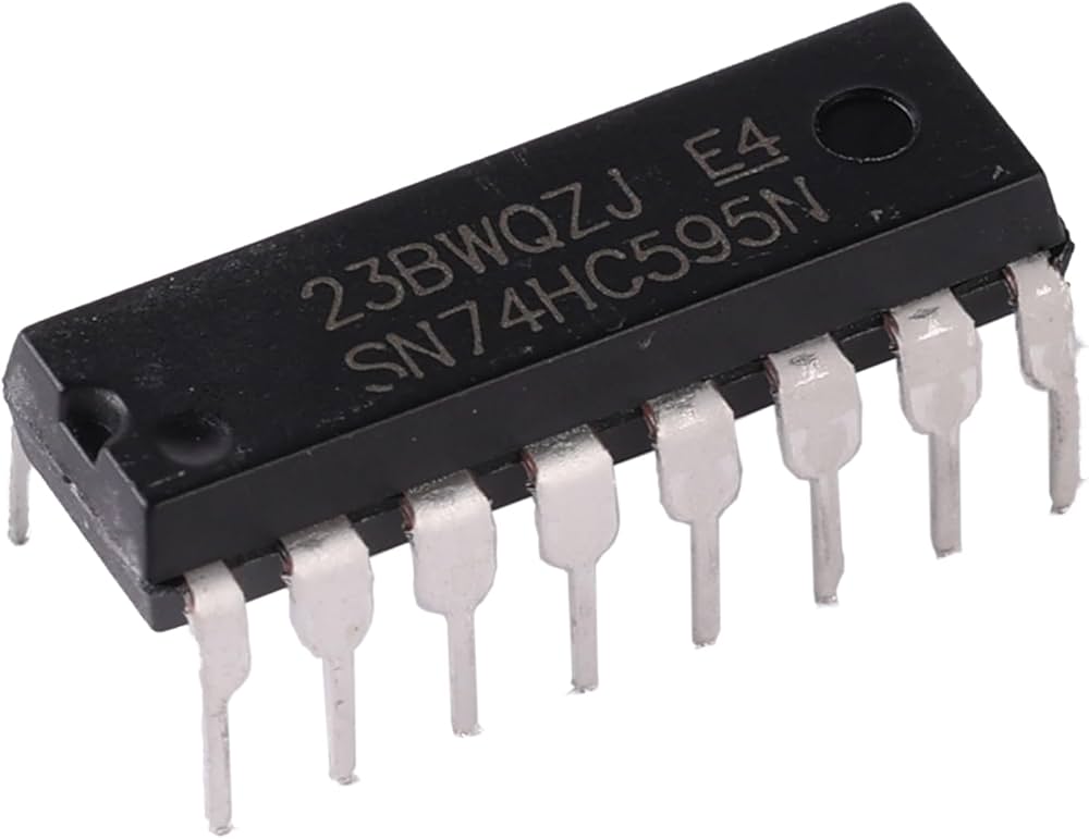
SN74HC595N is an 8-bit shift register with a serial input and a parallel output, designed using high-speed CMOS technology. It is commonly used for serial-to-parallel data conversion and is part of the 74HC (High-Speed CMOS) family.
Type: 8-bit Serial-In Parallel-Out Shift Register
Package: Typically available in a 16-pin DIP (Dual In-line Package) or SOIC package
Logic Family: 74HC (High-speed CMOS)
Operating Voltage (Vcc): 2V to 6V
High-Speed Operation: Fast data shifting and output latching
Low Power Consumption: Typical for CMOS logic circuits
Output Type: Three-state (high-impedance) output
Serial Input (DS): Receives serial data for the shift register.
Shift Register Clock (SH_CP): Controls the shifting of the data into the register.
Storage Register Clock (ST_CP): Controls the latching of data to the output pins.
Clear (MR): Active low reset input, clears the shift register.
Output Pins (Q0 - Q7): 8 parallel output pins (Q0 is the least significant bit).
Output Enable (OE): Active low input to disable/enable output drivers.
Supply Voltage (Vcc): 2V to 6V
Input Voltage (V_in): 0V to Vcc
Output Voltage (V_out): 0V to Vcc (depends on Vcc and load)
Input Current (I_in): Typically 1µA at 5V
Output Current (I_out): Can sink/source 6mA at Vcc = 5V
High-Level Output Voltage (V_OH): Vcc - 0.1V (at Vcc = 5V, I_out = -4mA)
Low-Level Output Voltage (V_OL): 0.1V (at Vcc = 5V, I_out = 4mA)
Shift Register Propagation Delay (t_plh/t_phl):
oMaximum: 20ns (at Vcc = 5V)
oTypical: 8ns (at Vcc = 5V)
Storage Register Propagation Delay (t_plh/t_phl):
oMaximum: 20ns (at Vcc = 5V)
oTypical: 8ns (at Vcc = 5V)
8-bit Serial-In Parallel-Out Shift Register: Allows conversion of serial data to parallel outputs.
Latch Mechanism: Storage register latches the data and transfers it to the outputs when the storage clock (ST_CP) is
Three-State Outputs: The outputs can be placed in a high-impedance state using the output enable pin (OE).
Clear Function (MR): Can clear all bits in the shift register to 0 with the clear input (active low).
Daisy-Chaining Capability: Multiple shift registers can be cascaded to expand the number of outputs.
Electrical Characteristics (at Vcc = 5V):
Operating Voltage (Vcc): 2V to 6V
Input Voltage (V_in): 0V to Vcc
Output Voltage (V_out): 0V to Vcc
Propagation Delay (t_plh/t_phl):
oMaximum: 20ns (shift and latch)
oTypical: 8ns
Input Current (I_in): Typically 1µA
Output Current (I_out): 6mA (sink or source)
Application Examples:
LED Drivers: Used to control large numbers of LEDs with a minimal number of control pins.
Display Systems: Ideal for controlling 7-segment displays.
Data Bus Expansion: Expanding the number of outputs or controlling peripherals with limited I/O.
Shift Registers for Serial Communication: Serial-to-parallel data conversion for devices like microcontrollers.