CD4011 is a quad 2-input NAND gate IC (integrated circuit)
Device Type: CMOS (Complementary Metal-Oxide-Semiconductor)
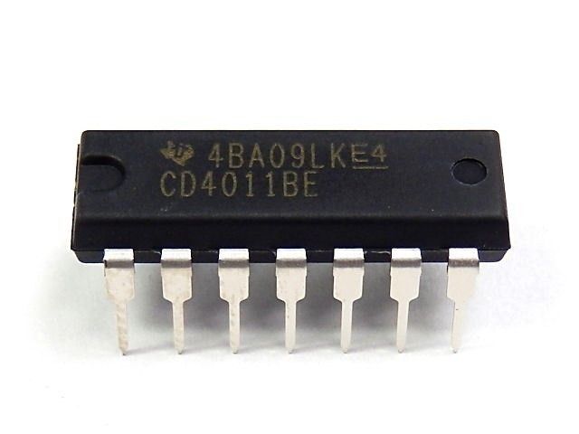
Package Types: Dual In-line Package (DIP), Surface-Mounted Package (SMD), etc.
Logic Gates: 4 x 2-input NAND gates
Operating voltage range: 3V to 15V
Recommended supply voltage: 5V or 9V
Input voltage range: 0V to Vcc
Logic High (V_IH): Typically 2V, minimum 1.5V
Logic Low (V_IL): Typically 0.8V, maximum 1.5V
Output Voltage (V_O):
Output voltage (High, V_OH): Typically Vcc - 1V (at 4mA output current)
Output voltage (Low, V_OL): Typically 0.4V (at 4mA output current)
Low (at V_IL): ±0.1µA
High (at V_IH): ±0.1µA
Output Current (I_O):
Low: 16mA maximum
High: 8mA maximum
Propagation delay from input to output is typically 30ns to 50ns (depending on voltage and load conditions).
Typically 25ns (at 5V supply voltage).
Typically 25ns (at 5V supply voltage).
Typically 1mA at 5V supply.
Maximum 10mA (under maximum load conditions).
Operating Temperature: Typically -40°C to 85°C.
Storage Temperature: Typically -65°C to 150°C.
Input Protection: The CD4011 has protection diodes to handle over-voltage conditions at its inputs.
Noise Immunity: Due to its CMOS technology, it has high noise immunity compared to TTL logic gates.